
Counter Timing Summary
The following figure shows the timing requirements for the gate and source input signals and the timing specifications for the output signals on your device.
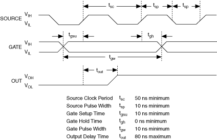
The gate and out signal transitions shown in the previous figure are referenced to the rising edge of the source signal. This timing diagram assumes that the counters are programmed to count rising edges. The same timing diagram, but with the source signal inverted and referenced to the falling edge of the source signal, applies when you program the counter to count falling edges.
The gate input timing parameters are referenced to the signal at the source input or to one of the internally generated signals on your device. The previous figure shows the gate signal referenced to the rising edge of a source signal. The gate must be valid (either high or low) for at least 10 ns before the rising or falling edge of a source signal so the gate can take effect at that source edge, as shown by tgsu and tgh. The gate signal is not required after the active edge of the source signal.
If you use an internal timebase clock, you cannot synchronize the gate signal with the clock. In this case, gates applied close to a source edge take effect either on that source edge or on the next one. This arrangement results in an uncertainty of one source clock period with respect to unsynchronized gating sources.
The output timing parameters are referenced to the signal at the source input or to one of the internally generated clock signals on your device. The previous figure shows the out signal referenced to the rising edge of a source signal. Any out signal state changes occur within 80 ns after the rising or falling edge of the source signal.
For information about the internal routing available on the DAQ-STC counter/timers, refer to Counter Parts in NI-DAQmx in the NI-DAQmx Help.