
Timing Signal Routing
The DAQ-STC provides a flexible interface for connecting timing signals to other devices or external circuitry. The S Series device uses the RTSI bus to interconnect timing signals between devices, and it uses the programmable function interface (PFI) pins on the I/O connector to connect the device to external circuitry. These connections are designed to enable the S Series device to both control and be controlled by other devices and circuits.
You can control the following timing signals internal to the DAQ-STC by an external source:
AI Sample Clock Timebase Signal
AO Sample Clock Timebase Signal
You also can control these timing signals by signals generated internally to the DAQ-STC, and these selections are fully software-configurable. The following figure shows an example of the signal routing multiplexer controlling the ai/SampleClock signal.
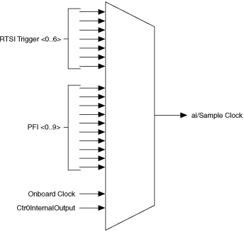
This figure shows that ai/SampleClock can be generated from a number of sources, including the external signals RTSI <0..6> (PCI and PXI buses only) and PFI <0..9> and the internal signals, Onboard Clock and Ctr0InternalOutput.
On PCI and PXI devices, many of these timing signals are also available as outputs on the PFI pins.
 | Note The Master Timebase signal can only be accepted as an external signal over RTSI. Refer to Device and RTSI Clocks for information about routing this signal. |